Difference between revisions of "Kimus 1a"
(→CDP1833CD: add romdump) |
|||
| (32 intermediate revisions by 2 users not shown) | |||
| Line 6: | Line 6: | ||
|ProjectPurpose=Infrastructure | |ProjectPurpose=Infrastructure | ||
}} | }} | ||
| − | + | Turn an old coin(quarters only) operated payphone into a doorbell/art-project for the building. | |
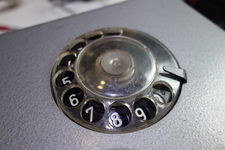
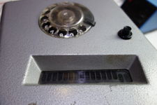
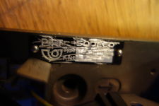
| − | + | Aquired an old 'Kimus 1a' aka 'PTT Sodeco TE 450'. This is an rotary-pulse-dial phone, the particular model seems to be one of the later ones and could be set to allow free calls. | |
| + | The payphone will be connected to an old Fritzbox 7170 which functions as an [https://en.wikipedia.org/wiki/Analog_telephone_adapter ATA] to connect to the VOIP-server. With this it can make and receive calls. | ||
| + | |||
| + | The VOIP-server will then redirect calls to spaces/renters in the building, it will only allow internal calls, or atleast no calls that cost money. 112 will be disabled to prevent prank-calls and due to reliability problems. | ||
| + | == Lock == | ||
| + | |||
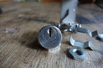
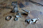
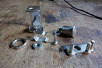
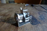
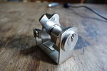
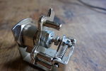
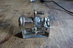
| + | The machine did not come with a key, but it was opened by lockpicking. | ||
| + | |||
| + | <gallery widths=150px> | ||
| + | File:Kimus1a-lock_00.jpg|Cylinder (number on the back) | ||
| + | File:Kimus1a-lock_03.jpg|Front of Cylinder | ||
| + | File:Kimus1a-lock_01.jpg|Disassembled | ||
| + | File:Kimus1a-lock_02.jpg|Disassembled, (the plate with the 3 pins at right-under moves the locking pin in the case) | ||
| + | File:Kimus1a-lock_04.jpg|Assembled | ||
| + | File:Kimus1a-lock_05.jpg|Assembled | ||
| + | File:Kimus1a-lock_06.jpg|Assembled (somehow the pin is crucial for opening) | ||
| + | File:Kimus1a-lock_07.jpg|Assembled | ||
| + | </gallery> | ||
| + | |||
| + | == Coin Mechanism == | ||
| + | |||
| + | This part will not be used in operation and is here only for documentation purposes. | ||
| + | |||
| + | * Validation is done mechanically by size and weight, by this mechanism: [[File:Kimus1_0010.jpg|50px]] | ||
| + | * The coin return button will return coins from this mechanism to the user | ||
| + | * When validated it will move towards the coin tracking system: [[File:Kimus1_109.jpg|50px]] | ||
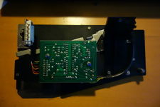
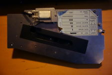
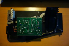
| + | * The PCB can be seen on: [[File:Kimus1_0102.JPG|50px]] and [[File:Kimus1_0103.JPG|50px]] | ||
| + | |||
| + | === Cointracker PCB === | ||
| + | <gallery widths=150px> | ||
| + | File:Kimus1_0102.JPG|Front | ||
| + | File:Kimus1_0103.JPG|Back | ||
| + | </gallery> | ||
| + | |||
| + | The two IC's are an MC14007UB and a MC14584BCL, seemingly dated on 1983. | ||
| + | * MC14007UB: Dual Complementary Pair Plus Inverter [[:File:MC14007UB-D.pdf|(datasheet)]] | ||
| + | * MC14584BCL: Hex Schmitt Trigger [[:File:mc14584bcp.pdf|(datasheet)]] | ||
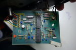
| + | == Mainboard == | ||
| + | |||
| + | === Mainboard PCB === | ||
| + | <gallery widths=150px> | ||
| + | File:Kimus1_0006.jpg|Front | ||
| + | File:Kimus_1_TE450-1.jpg|Back | ||
| + | </gallery> | ||
| + | |||
| + | The main board has a 27 single sided edge connetor, where the first 12 half is on the top and the remaining 15(!) on the bottom. Pin 13 is a key hole (on the mating connector is a pin missing | ||
| + | |||
| + | The following IC's are on the board | ||
| + | * MC14503BCL: Hex Non-Inverting 3-State Buffer ([[:File:MC14503BCP.pdf|datasheet]]) | ||
| + | * MC14017BCL: Decade counter ([[:File:MC14017BCL_to_MC14017BD.pdf|datasheet]]) | ||
| + | * MC14013B: dual type D flip−flop ([[:File:MC14013B-D.PDF|datasheet]]) | ||
| + | * MC1413L: High Voltage, High Current Darlington/Seven-Line Power Driver ([[:File:MC1413-D.PDF|datasheet]]) | ||
| + | * MC14042BCL: Quad Transparent Latch ([[:File:MC14042BCL_to_MC14042BD.pdf|datasheet]]) | ||
| + | * MC14049UB: Hex buffer/inverter ([[:File:MC14049UB-D.PDF|datasheet]]) | ||
| + | * MC14093BCL: Quad 2-Input NAND chmitt Trigger ([[:File:MC14093BCL.pdf|datasheet]]) | ||
| + | * HCMP1824D: Hughes Type HCMP 1824 wafers (32 x 8 Static RAMS)?posible ([[:File:P80862.pdf|datasheet]]) | ||
| + | * cd4047BCJ: Low power monostable / astable multivibrator ([[:File:cd4047bcj.pdf|datasheet]]) | ||
| + | * CDP1802CD: RCA 1802 Microprocessor ([https://en.wikipedia.org/wiki/RCA_1802 wikipedia], [[:File:cdp1802.pdf|datasheet]]) [http://www.cosmacelf.com/publications/data-sheets/ more datasheets] | ||
| + | * CDP1833CD: Mask Programmable ROM? ([[:File:DC1833CP.pdf|datasheet]]) | ||
| + | |||
| + | ==== CDP1833CD ==== | ||
| + | <gallery widths=150px> | ||
| + | File:cdp1833-back.jpg | ||
| + | File:cdp1833-front.jpg | ||
| + | </gallery> | ||
| + | |||
| + | ===== Dumping the ROM ===== | ||
| + | * https://groups.yahoo.com/neo/groups/cosmacelf/conversations/topics/19192 | ||
| + | * code http://www.avionline.com/CDP1833_Dumper.zip [[:File:CDP1833_Dumper.tar.gz]] | ||
| + | * dump: [[:File:romdump.txt]] | ||
| + | |||
| + | === Mainboard layout === | ||
| + | There is no layout made yet for this board but an example for the 1802 MCU was located in the DC1833 Rom datasheet. | ||
| + | [[File:CPUlayout.png|Example system layout]] | ||
| + | Inside the RCA MCU datasheet itself there is also an example available | ||
| + | |||
| + | rom dumping:https://www.nycresistor.com/2012/07/07/stick-a-straw-in-its-brain-and-suck-how-to-read-a-rom/ | ||
| + | |||
| + | === Settings === | ||
| + | <gallery widths=150px> | ||
| + | File:Kimus1_0013.jpg|Description field | ||
| + | </gallery> | ||
| + | |||
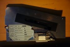
| + | The mainboard has four plugs with plastic keys that resemble numbers. On this board there are use a "0"(zero), "1", "2" and "5". | ||
| + | actualy they have 4 metal strips that can connect to a mating pin that with the other 3 plugs forms a 4bit like setting. | ||
| + | There is a sticker that somewhat describes what these should mean. | ||
| + | Its asummed that the lower left one describes: "Toesalg" in 5 cents increments | ||
| + | The lower right: "min. inworp" means minimal change. | ||
| + | The original setting was 0, 1 (zero toeslag, 1 coin to start), it was changed to say something like "zero starting fee, 1 coind for extra minutes" thus by experiment it resulted in free calling. Note, the phone does not recieve minutes signals, so the "toeslag" cant be applied or something (sorry my english: codeasm) | ||
| + | |||
| + | These "keys" have special shapes to form a indication of their value. It has been suggested that we could decode the meaning. We should take some detailed pictures of their shape. | ||
| + | |||
| + | == Bus == | ||
| + | |||
| + | The interconnections between the different boards. | ||
| + | <gallery widths=150px> | ||
| + | File:Kimus1a-20003.jpg | ||
| + | File:Kimus1a-Bus.png | ||
| + | </gallery> | ||
| + | |||
| + | == Bell & Dial system == | ||
| + | |||
| + | === PCB === | ||
| + | <gallery widths=150px> | ||
| + | File:Kimus1a-20004.jpg | ||
| + | File:Kimus1a-20005.jpg | ||
| + | File:Kimus1a-Bell_00.JPG | ||
| + | File:ring-dial-board.png | ||
| + | </gallery> | ||
| + | * C1: 1uF 250v [[:File:mkt1822.pdf|MKT1822]] | ||
| + | * R1: 558 Ohm | ||
| + | |||
| + | === Bell === | ||
| + | <gallery widths=150px> | ||
| + | File:Kimus1a-Bell_01.JPG | ||
| + | File:Kimus1a-Bell_02.JPG | ||
| + | </gallery> | ||
== Photos == | == Photos == | ||
| Line 20: | Line 136: | ||
File:Kimus1_0005.jpg | File:Kimus1_0005.jpg | ||
File:Kimus1_0006.jpg | File:Kimus1_0006.jpg | ||
| + | File:Kimus_1_TE450-1.jpg | ||
File:Kimus1_0007.jpg | File:Kimus1_0007.jpg | ||
File:Kimus1_0008.jpg | File:Kimus1_0008.jpg | ||
| Line 34: | Line 151: | ||
File:Kimus1_0019.jpg | File:Kimus1_0019.jpg | ||
File:Kimus1_0020.jpg | File:Kimus1_0020.jpg | ||
| + | File:Kimus1 107.jpg | ||
| + | File:Kimus1 109.jpg | ||
| + | File:Kimus1_0100.JPG | ||
| + | File:Kimus1_0101.JPG | ||
| + | File:Kimus1_0102.JPG | ||
| + | File:Kimus1_0103.JPG | ||
| + | File:Kimus1a-20003.jpg | ||
| + | File:Kimus1a-20004.jpg | ||
| + | File:Kimus1a-20005.jpg | ||
| + | File:Kimus1a-20006.jpg | ||
| + | File:Kimus1a-20007.jpg | ||
| + | File:Kimus1a-20008.jpg | ||
</gallery> | </gallery> | ||
Latest revision as of 23:17, 19 February 2017
| Projects | |
|---|---|
| |
| Participants | CodeAsm, Erwin-c64, Webmind |
| Skills | pots, electronics, voip |
| Status | Active |
| Niche | Electronics |
| Purpose | Infrastructure |
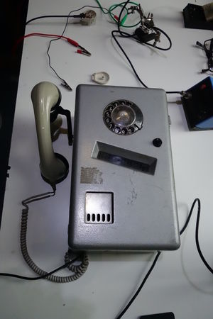
Turn an old coin(quarters only) operated payphone into a doorbell/art-project for the building.
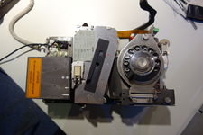
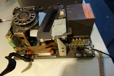
Aquired an old 'Kimus 1a' aka 'PTT Sodeco TE 450'. This is an rotary-pulse-dial phone, the particular model seems to be one of the later ones and could be set to allow free calls.
The payphone will be connected to an old Fritzbox 7170 which functions as an ATA to connect to the VOIP-server. With this it can make and receive calls.
The VOIP-server will then redirect calls to spaces/renters in the building, it will only allow internal calls, or atleast no calls that cost money. 112 will be disabled to prevent prank-calls and due to reliability problems.
Contents
Lock
The machine did not come with a key, but it was opened by lockpicking.
Coin Mechanism
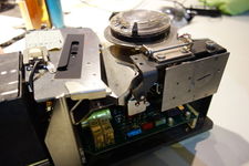
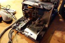
This part will not be used in operation and is here only for documentation purposes.
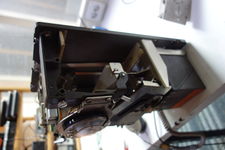
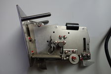
- Validation is done mechanically by size and weight, by this mechanism:

- The coin return button will return coins from this mechanism to the user
- When validated it will move towards the coin tracking system:

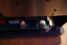
- The PCB can be seen on:
and
Cointracker PCB
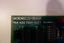
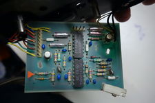
The two IC's are an MC14007UB and a MC14584BCL, seemingly dated on 1983.
- MC14007UB: Dual Complementary Pair Plus Inverter (datasheet)
- MC14584BCL: Hex Schmitt Trigger (datasheet)
Mainboard
Mainboard PCB
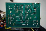
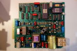
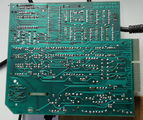
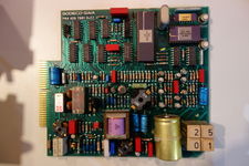
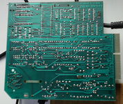
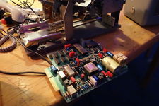
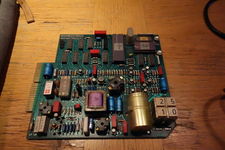
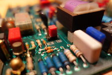
The main board has a 27 single sided edge connetor, where the first 12 half is on the top and the remaining 15(!) on the bottom. Pin 13 is a key hole (on the mating connector is a pin missing
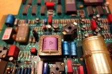
The following IC's are on the board
- MC14503BCL: Hex Non-Inverting 3-State Buffer (datasheet)
- MC14017BCL: Decade counter (datasheet)
- MC14013B: dual type D flip−flop (datasheet)
- MC1413L: High Voltage, High Current Darlington/Seven-Line Power Driver (datasheet)
- MC14042BCL: Quad Transparent Latch (datasheet)
- MC14049UB: Hex buffer/inverter (datasheet)
- MC14093BCL: Quad 2-Input NAND chmitt Trigger (datasheet)
- HCMP1824D: Hughes Type HCMP 1824 wafers (32 x 8 Static RAMS)?posible (datasheet)
- cd4047BCJ: Low power monostable / astable multivibrator (datasheet)
- CDP1802CD: RCA 1802 Microprocessor (wikipedia, datasheet) more datasheets
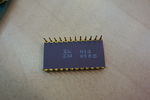
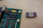
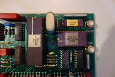
- CDP1833CD: Mask Programmable ROM? (datasheet)
CDP1833CD
Dumping the ROM
- https://groups.yahoo.com/neo/groups/cosmacelf/conversations/topics/19192
- code http://www.avionline.com/CDP1833_Dumper.zip File:CDP1833_Dumper.tar.gz
- dump: File:romdump.txt
Mainboard layout
There is no layout made yet for this board but an example for the 1802 MCU was located in the DC1833 Rom datasheet.
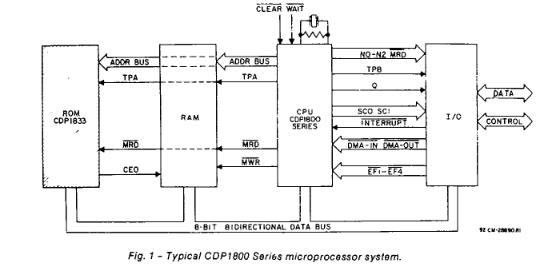 Inside the RCA MCU datasheet itself there is also an example available
rom dumping:https://www.nycresistor.com/2012/07/07/stick-a-straw-in-its-brain-and-suck-how-to-read-a-rom/
Settings
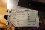
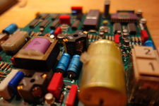
The mainboard has four plugs with plastic keys that resemble numbers. On this board there are use a "0"(zero), "1", "2" and "5". actualy they have 4 metal strips that can connect to a mating pin that with the other 3 plugs forms a 4bit like setting. There is a sticker that somewhat describes what these should mean. Its asummed that the lower left one describes: "Toesalg" in 5 cents increments The lower right: "min. inworp" means minimal change. The original setting was 0, 1 (zero toeslag, 1 coin to start), it was changed to say something like "zero starting fee, 1 coind for extra minutes" thus by experiment it resulted in free calling. Note, the phone does not recieve minutes signals, so the "toeslag" cant be applied or something (sorry my english: codeasm)
These "keys" have special shapes to form a indication of their value. It has been suggested that we could decode the meaning. We should take some detailed pictures of their shape.
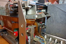
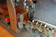
Bus
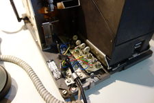
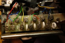
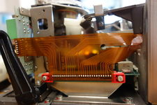
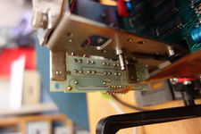
The interconnections between the different boards.
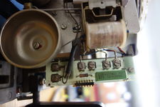
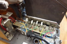
Bell & Dial system
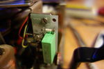
PCB
- C1: 1uF 250v MKT1822
- R1: 558 Ohm
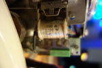
Bell
Photos
Known issues
- The ring-power from the fritzbox is rather low, due to this the bell isn't too audible.
- The lock needs to be replaced as we don't have a key for the device.

